Construction of SCR (Thyristor): Internal Arrangement, Layers, Junctions and Working
Ch. Devi Lal Government Polytechnic, Nathusari Chopta › Diploma in Engineering (Polytechnic) › Electrical Engineering › Semester 5
Construction of SCR (Thyristor): Internal Arrangement, Layers, Junctions and Working
An ordinary switch in your home has to be pressed by hand every time. In industry, we need switches that work by themselves, very fast and without any moving part, to control motors, heaters, lamps and battery chargers. Such electronic switches are called thyristors. The most important thyristor is the SCR (Silicon Controlled Rectifier).
The SCR is one of the most important members of the semiconductor family and has largely replaced older power control devices such as thyratrons and mechanical contactors in many applications. Its construction is simple: it is a piece of silicon with four layers and three junctions. The first SCR was developed in Bell Laboratories (USA) in 1956, and General Electric (GE) introduced the first commercial SCR soon after, in 1957.
In this note you will first learn what a thyristor is. Then you will study the construction of an SCR in detail: its four layers, three junctions, terminals, symbol, internal arrangement and packages. After that you will learn how it works, its V-I characteristics, how it is turned ON (triggering) and OFF (commutation), how it is protected, and why it needs a heat sink. If you want to revise P-type and N-type material first, read Semiconductor Fundamentals.
1. What Is a Thyristor?
Definition: A thyristor is a semiconductor switching device made of alternate P and N layers (usually four layers, P-N-P-N). It can be turned ON by a small control signal, and once it is ON, it keeps conducting until the current is reduced.
Examples: SCR, DIAC, TRIAC, GTO (gate turn-off thyristor).
Analogy (not exact): A thyristor works like a door latch. A small push (the gate signal) opens the latch, and the door then stays open by itself until the flow through it stops.
Important point: A thyristor is used only as a switch (fully ON or fully OFF). It is not used as an amplifier.
Exam tip: “Name any two members of the thyristor family” has been asked as a 1-mark question.
2. Classification of Thyristors
Thyristors can be grouped by the direction of current they allow, by the number of terminals and by the way they are turned ON or OFF. The common types are given below (textbook classification).
| Type | Terminals | Direction of conduction | How it is controlled |
|---|---|---|---|
| SCR (Silicon Controlled Rectifier) | 3 (anode, cathode, gate) | One direction (unidirectional) | Turned ON by a gate pulse; turned OFF by commutation |
| LASCR (Light Activated SCR) | 3 (or 2) | One direction | Turned ON by light falling on it |
| GTO (Gate Turn-Off thyristor) | 3 | One direction | Turned ON and also turned OFF by gate pulses |
| DIAC | 2 | Both directions (bidirectional) | Turns ON when the voltage reaches its breakover value |
| TRIAC | 3 (MT1, MT2, gate) | Both directions | Turned ON by a gate pulse of either polarity |
| SCS (Silicon Controlled Switch) | 4 | One direction | Small-power device with two gates |
Remember: SCR is unidirectional. DIAC and TRIAC are bidirectional.
Exam tip: “Classification of thyristors” has been asked as a short note.
3. Construction of SCR (Internal Arrangement)
Definition: An SCR is a three-terminal, four-layer, three-junction, unidirectional semiconductor switch. It conducts from anode to cathode only after a small positive signal is given to the gate.
3.1 Four layers and three junctions
Four layers of silicon, P-N-P-N, are joined one after another. This gives three junctions, J1, J2 and J3. The anode is connected to the outer P layer, the cathode to the outer N layer, and the gate to the inner P layer near the cathode (Fig. 1).
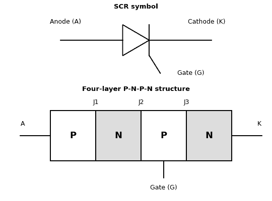 Fig. 1: SCR symbol and its four-layer P-N-P-N structure
Diagram in words: The top part shows the SCR symbol: a triangle pointing from the anode to the cathode, with the gate line coming out near the cathode. The lower part shows four blocks in a row, P, N, P and N, with the junctions J1, J2 and J3 between them. The anode is joined to the first P block, the cathode to the last N block and the gate to the second P block.
| Layer | Type | Doping and thickness (typical) | Connected to |
|---|---|---|---|
| P1 (outer P layer) | P | Heavily doped | Anode (A) |
| N1 (inner N layer, N-base) | N | Lightly doped and the thickest layer | Nothing (internal layer) |
| P2 (inner P layer, P-base) | P | Moderately doped | Gate (G) |
| N2 (outer N layer) | N | Heavily doped and thin | Cathode (K) |
Why the layers are different: The thick, lightly doped N1 layer decides how much voltage the SCR can block, so high-voltage SCRs have a thicker N1 layer. The thin, heavily doped N2 layer supplies plenty of charge carriers when the SCR is ON. The gate is joined to P2 so that a small gate current can easily start conduction at the cathode end.
3.2 The three junctions and their job
| Junction | Between layers | Role |
|---|---|---|
| J1 | P1 and N1 (near the anode) | Forward biased when the anode is positive. Blocks the main reverse voltage when the anode is negative. |
| J2 | N1 and P2 (middle) | The main blocking junction. It is reverse biased in the forward blocking mode, and it holds the forward voltage until the SCR is triggered. |
| J3 | P2 and N2 (near the cathode) | Forward biased when the anode is positive. The gate current forward biases it and starts conduction. |
Remember: J2 is the junction that blocks the voltage in the forward direction. J1 blocks it in the reverse direction.
3.3 Terminals and symbol
- Anode (A): taken from the outermost P layer. It is the positive terminal.
- Cathode (K): taken from the outermost N layer. It is the negative terminal.
- Gate (G): taken from the inner P layer, near the cathode. It is the control terminal.
The SCR symbol is similar to a diode symbol, with one extra line for the gate. The arrow points from the anode to the cathode, which is the direction of conventional current.
3.4 Physical construction and packages
In a real SCR, the silicon is a thin round wafer (pellet) made by a diffusion process. The wafer is fixed to a disc of molybdenum or tungsten, which expands about as much as silicon does, and this disc is joined to a thick copper base. Metal contacts are made for the anode, the cathode and a small gate contact, and the whole assembly is sealed in a metal-ceramic or plastic case. The case is built so that the heat from the wafer can flow out easily (Fig. 2).
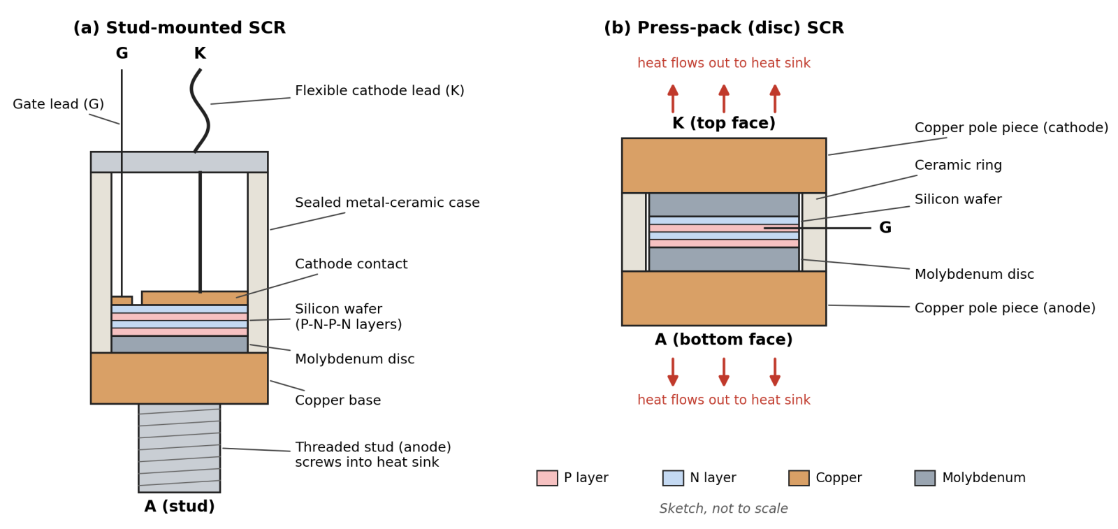 Fig. 2: Physical construction of stud-mounted and press-pack SCRs (sketch, not to scale)
Diagram in words: On the left, a stud-mounted SCR is shown: a threaded copper stud at the bottom (the anode), a sealed case in the middle, and a flexible cathode lead and a thin gate lead coming out of the top. On the right, a press-pack (disc) SCR is shown as a flat round disc with a metal face on the top (cathode) and a metal face on the bottom (anode), and a small gate lead on the side. A cut-away inside both shows the silicon wafer fixed on the molybdenum disc.
| Package | Power level | How it is used |
|---|---|---|
| Stud-mounted | Low to medium | The threaded stud (usually the anode) is screwed into a heat sink. |
| Press-pack (disc or “hockey puck”) | High | The disc is clamped between two heat sinks, so heat is removed from both faces. |
| Plastic (for example TO-220, TO-92) | Small | Used in small circuits such as light dimmers and alarms. The pin order differs between makers, so check the data sheet. |
Important point: The gate only starts the conduction and carries very little power. The load current flows from anode to cathode.
SCR compared with a diode: Both conduct in one direction only. A diode has two layers and one junction and starts conducting as soon as it is forward biased. An SCR has four layers and three junctions and, even when it is forward biased, it conducts only after the gate signal (or breakover) turns it ON.
Applications:
- Controlled rectifiers and battery chargers
- Speed control of DC and universal motors
- Inverters, choppers and UPS
- Static switches and protection circuits
Exam tip: Facts about the SCR structure have been asked as MCQs: “four layer, three junction”, “P-N-P-N device” and “unidirectional switch”.
4. Working of an SCR
An SCR can work in three modes.
(a) Forward blocking mode (OFF state): The anode is positive and the cathode is negative, but the gate is open. J1 and J3 are forward biased, but J2 is reverse biased. So only a very small leakage current flows. The SCR acts like an open switch (see the junction roles in Section 3.2).
(b) Forward conduction mode (ON state): A small positive gate current is given while the anode is positive. The gate current makes J2 break down at a much lower voltage than normal, and the SCR turns ON. Now all three junctions conduct. The voltage across the SCR falls to a small value (about 1 V to 1.5 V, textbook value), and the load current is limited only by the load. The gate loses control after this point. Even if the gate signal is removed, the SCR stays ON.
(c) Reverse blocking mode: The anode is negative and the cathode is positive. J1 and J3 are reverse biased and J2 is forward biased. Only a small reverse leakage current flows. The SCR blocks the current in this direction.
Turning OFF: A gate signal cannot turn off an ordinary SCR. It turns OFF only when the anode current falls below the holding current (or the anode voltage is reversed). This is called commutation (Section 10).
Exam tip: “Explain the working of SCR” has been asked as a 4-mark short question.
5. V-I Characteristics of an SCR
The V-I characteristic is a graph of anode current (IA) against anode-to-cathode voltage (VAK) (Fig. 3).
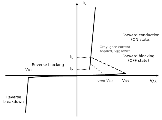 Fig. 3: V-I characteristics of an SCR (sketch, not to scale)
Diagram in words: The horizontal axis is the anode-to-cathode voltage and the vertical axis is the anode current. On the right, the curve stays almost flat (forward blocking) until the forward breakover voltage VBO. It then jumps along a dashed line to a steep, almost vertical line (forward conduction). The holding current IH and the larger latching current IL are marked on the current axis. A grey curve shows that a gate current makes the breakover voltage lower. On the left, the curve is almost flat (reverse blocking) until the reverse breakdown voltage, where the current falls sharply downward.
Explanation of the graph:
- Forward blocking region: With gate open, only a tiny leakage current flows as VAK increases.
- Forward breakover voltage (VBO): When VAK reaches VBO, the SCR turns ON by itself, and the voltage across it falls (the dashed part is the negative resistance region). This is not a normal way to turn on an SCR, because it can damage the device.
- Forward conduction region: The curve is almost vertical. The current rises very fast and the voltage drop stays small.
- Effect of gate current: If gate current is given, the SCR turns ON at a voltage lower than VBO. A larger gate current gives a lower turn-on voltage.
- Reverse blocking region: In the reverse direction, only a small leakage current flows until the reverse breakdown voltage is reached. Beyond that, the current rises suddenly and the SCR can be damaged.
6. Latching Current and Holding Current
| Point | Latching current (IL) | Holding current (IH) |
|---|---|---|
| Meaning | Minimum anode current needed to keep the SCR ON just after the gate signal is removed | Minimum anode current needed to keep the SCR ON once it is already conducting |
| Related to | Turn-on process | Turn-off process |
| If the current is lower | SCR returns to OFF when the gate pulse ends | SCR turns OFF |
| Value | Larger | Smaller |
Remember: IL is greater than IH. In many SCRs, IL is about two to three times IH (textbook value).
Exam tip: These points have been asked as MCQ or True/False: latching current is related to the turn-on process; the SCR turns off when anode current falls below a certain value; latching current is more than holding current (True/False).
7. Two-Transistor Analogy of an SCR
The four-layer P-N-P-N structure can be imagined as two transistors joined together: a PNP transistor Q1 (layers P-N-P at the top) and an NPN transistor Q2 (layers N-P-N at the bottom). The middle N and P layers are shared (Fig. 4).
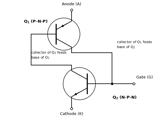 Fig. 4: Two-transistor analogy of an SCR
Diagram in words: A PNP transistor Q1 is placed above an NPN transistor Q2. The emitter of Q1 is the anode and the emitter of Q2 is the cathode. The collector of Q1 is joined to the base of Q2, and this point is also the gate. The collector of Q2 is joined to the base of Q1. This cross connection gives the regenerative (self-increasing) action.
Connections:
- The emitter of Q1 is the anode, and the emitter of Q2 is the cathode.
- The collector of Q1 is connected to the base of Q2. The gate is also connected here.
- The collector of Q2 is connected to the base of Q1.
Working:
- A positive gate current gives base current to Q2, and Q2 starts conducting.
- The collector current of Q2 is the base current of Q1, so Q1 starts conducting.
- The collector current of Q1 goes back as more base current to Q2.
- This feedback keeps increasing the currents very fast (regenerative action), until both transistors are fully ON. The SCR is now latched ON, and the gate has no further control.
Important point: The regeneration starts when the sum of the current gains of the two transistors reaches 1 (textbook statement).
Exam tip: “Draw and explain two transistor analogy of SCR” has been asked as a 4-mark question.
8. Methods of Triggering an SCR
Definition: Triggering means turning ON an SCR, that is, making it change from the OFF state to the ON state. An SCR can be triggered in the following ways.
| Method | How it turns ON the SCR | Use |
|---|---|---|
| 1. Forward voltage (breakover) triggering | The anode voltage is raised above VBO | Not used in practice; can damage the SCR |
| 2. Gate triggering | A small positive current is given to the gate | The normal and preferred method |
| 3. dv/dt triggering | A very fast rise of anode voltage charges the junction capacitance and works like a gate current | Unwanted (false triggering); avoided by a snubber |
| 4. Temperature triggering | High temperature increases the leakage current, which turns the SCR ON | Unwanted; avoided by a heat sink |
| 5. Light triggering | Light falls on the junction of a LASCR and creates charge carriers | Used in light-activated devices and in isolated triggering |
Types of gate triggering:
- DC gate triggering: A steady DC voltage is applied to the gate.
- AC gate triggering: An AC voltage, often shifted in phase by an R-C network, is applied to the gate. The phase shift sets the firing angle.
- Pulse triggering: A short pulse (for example from a UJT oscillator) is applied to the gate. This is the best method because it gives less gate power loss and sharp control.
Exam tip: Triggering of an SCR has been asked as a 4-mark question in every one of the previous papers (“define triggering and explain any two methods”, “explain the different methods” and “write two methods”).
9. dv/dt and di/dt Protection (Snubber Circuit)
dv/dt protection: If the anode voltage rises very quickly, a current flows through the internal junction capacitance of the SCR. This acts like a gate current and can turn on the SCR by mistake. To avoid this, a snubber circuit is connected across the SCR. It is a resistor Rs in series with a capacitor C (Fig. 5). The capacitor slows down the rise of voltage across the SCR. The resistor limits the discharge current of the capacitor when the SCR turns ON, and it also reduces oscillations.
di/dt protection: When the SCR turns ON, conduction starts in a small area near the gate and then spreads. If the anode current rises too fast, this small area becomes very hot and the SCR can be damaged. To avoid this, a small inductor L is connected in series with the SCR. The inductor limits the rate of rise of current.
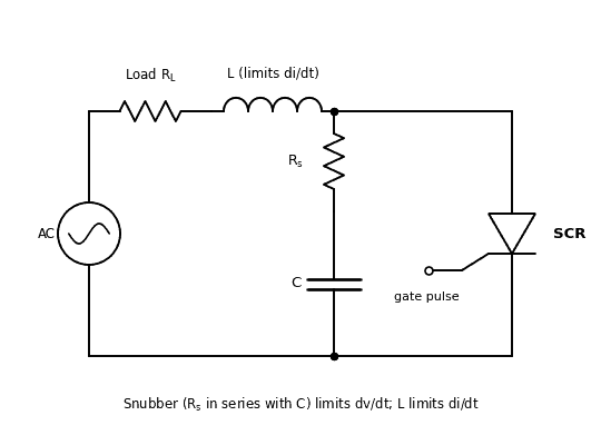 Fig. 5: SCR protection: series inductor (di/dt) and R-C snubber (dv/dt) (circuit sketch)
Diagram in words: An AC source feeds a load resistor and a series inductor L. The SCR is connected after the inductor. A resistor Rs in series with a capacitor C is connected across the SCR (from its anode to its cathode). The gate pulse comes from a separate trigger circuit.
Exam tip: The use of a snubber circuit has been asked as an MCQ: “protection of SCR”.
10. Commutation of Thyristors
Definition: Commutation is the process of turning OFF a conducting thyristor. To turn it off, the anode current must be brought below the holding current, and the SCR must then be kept reverse biased for a short time (the turn-off time) so that it can block the forward voltage again.
Commutation is necessary because the gate cannot turn off an ordinary SCR.
| Point | Natural (line) commutation | Forced commutation |
|---|---|---|
| Where used | AC circuits | DC circuits (choppers and inverters) |
| How the SCR turns OFF | The AC supply current falls to zero at the end of each half cycle, and the voltage then reverses | An extra circuit with a charged capacitor and an inductor pushes the current to zero or applies a reverse voltage |
| Extra circuit needed | No | Yes |
| Examples | Controlled rectifiers, AC voltage controllers | Choppers, inverters |
Note: In textbooks, forced commutation is divided into several classes (for example self commutation, resonant pulse, complementary, auxiliary and external pulse commutation). You should learn the general idea and one example for the exam.
Exam tip: “Define commutation” has been asked as a 1-mark question.
11. Heat Sinks for Thyristors
Definition: A heat sink is a metal piece with fins, fixed to a device to take heat away from it and give that heat to the air.
Why it is needed: An SCR is not a perfect switch. A small voltage drop remains across it when it is ON, so power (voltage drop × current) is lost as heat. If the junction temperature goes above the allowed limit, the SCR can fail or turn on by mistake.
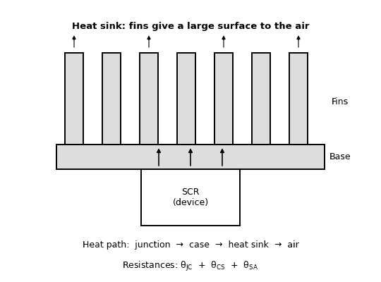 Fig. 6: Thyristor on a finned heat sink (sketch, not to scale)
Diagram in words: A block marked SCR is fixed under a wide metal base plate. Many vertical fins stand on the base plate. Arrows go upward from the SCR through the base and out of the fins into the air. A line below the figure shows the heat path: junction, case, heat sink, air, with the thermal resistances θJC, θCS and θSA.
Selection of a heat sink: Heat flows from the junction to the case, from the case to the heat sink and from the heat sink to the air. Each step has a thermal resistance, measured in °C per watt (°C/W). The junction temperature is:
TJ = TA + P × (θJC + θCS + θSA)
Here TJ is the junction temperature, TA is the ambient (surrounding) temperature, P is the power lost in the device in watts, θJC is the junction-to-case resistance, θCS is the case-to-sink resistance and θSA is the sink-to-air resistance. TJ must not exceed the maximum value given in the data sheet. The required heat sink resistance is:
θSA = (TJ(max) − TA) / P − θJC − θCS
A heat sink with θSA equal to or lower than this value should be chosen. These are standard textbook relations, and the data of the device must be taken from its data sheet.
Points to consider:
- Power lost in the device and the maximum junction temperature.
- Ambient temperature.
- Material: aluminium is common because it is light and conducts heat well; copper is better but costly.
- More fins and larger surface area give lower θSA. A fan (forced cooling) lowers it further.
- A flat, clean contact surface with thermal paste lowers θCS.
Note (safety): The case or stud of many thyristors is connected to the anode, so the heat sink can be at a live voltage. Use an insulating washer where needed and do not touch the heat sink when the circuit is ON.
Exam tip: “What is the role of heat sinks?” has been asked as a 1-mark question, and “Heat sink for thyristor” as a short note.
Everyday Examples to Remember
- A door latch: a small push opens it and it stays open (SCR turn-on and latching).
- A water tap that you can open with a button but can close only by stopping the water flow (an SCR cannot be turned off by the gate).
- A cooling fin on a scooter engine or a CPU cooler: the fins take heat away (heat sink).
MCQ and True/False Facts
- An SCR is a unidirectional switch.
- An SCR is a four-layer, three-junction, P-N-P-N device.
- Latching current is related to the turn-on process of the SCR.
- Latching current is more than holding current: True.
- An SCR turns off when the anode current falls below the holding current.
- A snubber circuit is used for the protection of an SCR.
- SCR, DIAC and TRIAC are members of the thyristor family.
- The gate of an SCR is connected to the inner P layer (P2).
- J2 is the junction that blocks the forward voltage of an SCR.
Important Questions for Examinations
Short Answer Questions
- What is a thyristor? Explain the classification of thyristors.
- Explain the working of an SCR.
- Define latching current and holding current. How are they different?
- Draw and explain the two-transistor analogy of an SCR.
- Define triggering. Explain any two methods of triggering of an SCR.
- What is a snubber circuit? Explain the dv/dt and di/dt protection of an SCR.
- What is the role of a heat sink? How is a heat sink selected for a thyristor?
Long Answer Questions
- Explain the construction, working principle and V-I characteristics of an SCR.
- What is commutation? Explain natural commutation and forced commutation of thyristors.
Quick Revision
- SCR: P-N-P-N, 3 junctions, 3 terminals (A, K, G), unidirectional.
- Anode: outer P layer. Cathode: outer N layer. Gate: inner P layer near the cathode.
- J2 blocks forward voltage; J1 blocks reverse voltage.
- Packages: stud-mounted (medium power), press-pack (high power), plastic (small power).
- Gate turns ON the SCR; the gate cannot turn it OFF.
- IL > IH. IL is for turn-on; IH is for turn-off.
- Two-transistor analogy: PNP + NPN with cross connection gives regeneration.
- Triggering methods: forward voltage, gate, dv/dt, temperature, light. Gate (pulse) triggering is preferred.
- Snubber (R + C) protects against dv/dt. Series inductor protects against di/dt.
- Natural commutation is used in AC. Forced commutation is used in DC.
- Heat sink: TJ = TA + P(θJC + θCS + θSA).
Frequently Asked Questions
Why is the SCR called a four-layer device?
Because it is made of four alternate layers of P-type and N-type silicon (P-N-P-N), which form three junctions.
Which junction blocks the voltage in the forward direction?
Junction J2. It is reverse biased when the anode is positive and the gate is open, so only a leakage current flows until the SCR is triggered.
Why is the gate connected to the inner P layer?
A small positive gate current into the P2 layer forward biases junction J3 and lets J2 break down at a low voltage, so a small control signal can turn the SCR ON.
What material is used to make an SCR?
Silicon. It handles higher temperature and voltage than germanium, and its leakage current is much lower.
Related Topics to Study Next
For more detail on the characteristics of the SCR, read SCR: Construction, Working and V-I Characteristics (Detailed). For protection methods, read Thyristor (SCR): Protection Methods and Technologies.
Next topics: DIAC and TRIAC; UJT and relaxation oscillator; Applications of SCR, DIAC and TRIAC; Single phase controlled rectifiers (Unit II).
Conclusion
The SCR is the basic thyristor. It is built from four layers of silicon (P-N-P-N) with three junctions, and its three terminals are the anode, the cathode and the gate. A small gate pulse turns it ON, and it stays ON until the current falls below the holding current. To use an SCR safely, we must trigger it properly, protect it from fast changes in voltage and current, turn it off by commutation and keep it cool with a heat sink.
More notes in Industrial Electronics & Control of Drives
- Cyclo-Converter Controlled AC Drives and Electric Braking
- AC Drives: Phase Control, Variable Frequency and Constant V/f Control
- DC Drives: Speed Control, Half-Wave, Full-Wave and Chopper Drives
- Electric Drives: Concept, Block Diagram and Advantages
- Thyristor (SCR) - Protection Methods and Technologies
- SCR : Construction, Working and V-I characterstics - Detailed
Comments (0)
Sign in or create an account to leave a comment.
No comments yet.